Reinforcing Wafer-Level Packaging with Novel Temporary Bonding / Debonding Technology
Brewer Science
Wafer-level packaging is an innovative technology for integrated circuits and electronics as it helps streamline the fabrication process. Its use in major application areas, like smartphones, has cemented its position as an effective technique for large-scale production, especially with the market’s demand for enhanced performance and flexibility. When it comes to handling thin substrates, one key procedure that stands out as a technology enabling process is temporary bonding / debonding. However, these techniques require particular materials that can meet the diverse packaging design requirements. Here, we will discuss what wafer-level packaging actually is, and how a novel temporary bonding / debonding system enables it effectively.
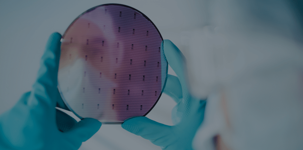
Figure 1. A wafer holding an array of microdevices. (Brewer Science)
Conventionally, the electronic packaging process flow involves dicing the wafer into small individual units, and then packaging them, separately. This can result in relatively large package sizes compared to the die size. Furthermore, with the continuous increase in integration complexity and in demand for high performance, high functionality, low power consumption, and small form factor, it has become quite challenging for such a packaging technology to fully meet modern requirements. This has led to the rise of an alternative packaging process called wafer-level packaging (WLP).
What is wafer-level packaging?
WLP is characterised by packaging the dies while they are still on the wafer. In other words, the steps of dicing and packaging of the traditional packaging process are reversed. Protective layers and electrical connections are introduced to the substrate prior to the dicing step. Doing so enables further reduction in chip size, more streamlined fabrication, and easier testing of chip functionality. WLP also helps bring the packaging cost down while allowing higher levels of integration.
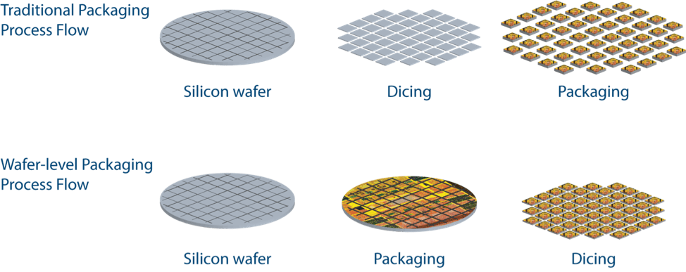
Figure 2. The difference between traditional packaging and wafer-level packaging process flows. (Brewer Science)
Starting from the standard wafer-level packaging, a remarkable evolution has taken place with the development of enhanced versions of WLP, including wafer-level chip-scale packaging (WLCSP) and fan-out wafer-level packaging (FOWLP).
Wafer-level chip-scale packaging (WLCSP)
WLCSP’s cost/performance ratio has enabled it to be today’s most common packaging technique, especially with the removal of the package substrate. However, its small die size is a limiting factor for its number of I/O.
Fan-out wafer-level packaging (FOWLP)
FOWLP has been widely developed with the main aim of circumventing the issue of limited external contacts. By fanning out interconnections to external locations, FOWLP can bring about a rise in I/O density while maintaining a small package footprint and low power consumption.
Other WLP technologies, such as package-on-package (PoP) and through-silicon via (TSV), are effective techniques for integration but suffer from difficulties in achieving low manufacturing cost, low power consumption, and reduced form factor.
Generally, WLP technologies are faced with the challenge of handling thin substrates during manufacturing. As a result, they require particular solutions that can facilitate the configuration and fabrication of complex packaging setups. One vital system that fits these criteria is temporary bonding /debonding (TB/DB).
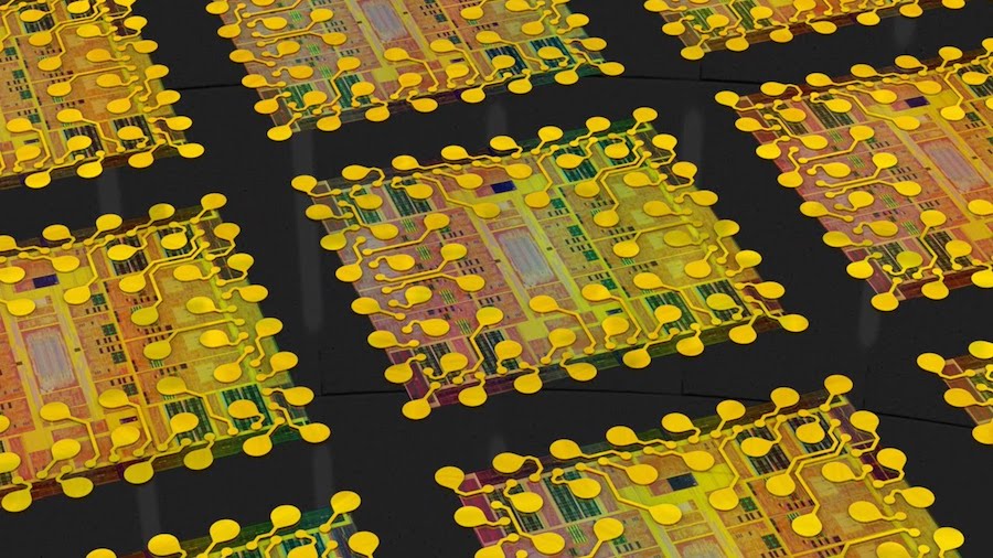
Figure 3. Array of microdevices during a fan-out wafer-level packaging process. (Brewer Science)
Temporary bonding-debonding (TB/DB) process
In handling thin and fragile substrates, TB/DB is an instrumental process that provides mechanical support for the wafers, especially for 3-dimensional integrated circuits, FOWLP wafers, and power devices. Basically, a device substrate is bonded to a rigid carrier by means of a temporary bonding adhesive material. The latter can also use a release layer, which helps separate the bonded structure upon the completion of the process, depending on the debond method. Ideally, a well-attached wafer should be stable against possible lateral wafer movement and vertical deformation of the bonding material.
For that reason, selecting the right bonding/debonding materials is a crucial aspect of the TB/DB process, especially with the rise of diversity in packaging designs that requires highly customised and specific materials.
Material selection for temporary bonding/debonding
In order for bonding materials to maintain minimal vertical deformation during die placement and minimal die shift during over-moulding, they have to have high melt viscosity and high thermal stability. This is particularly important due to the mismatch between the coefficients of thermal expansion (CTEs) of the carrier and substrate material. Bonding materials have to also be customised in a way that minimizes stress effects in stacked wafers, where warpage might occur, resulting in issues of alignment and handling. They should have sufficient adhesion to the substrate material to be able to tolerate such stresses.
One material category that has been commonly used as temporary bonding material is thermoplastic polymers. With adjustable thermo-mechanical stability and suitable properties, thermoplastics can enable the handling of very thin wafers against deformation and warpage. However, their limitation lies at the impasse of bonding temperature vs processing temperature. Low-temperature bonding materials can help increase throughput, reduce substrate damage, and lower energy consumption. Yet, subjecting them to high temperatures during processing would cause them to lose melt viscosity and thus mechanical stability as they soften and begin to behave as liquid rather than solid. This may result in serious wafer deformation and lack of bond stability under the effects of compressive and tensile stresses.
The best solution for TB/DB processes
To tackle the issue of temperature compatibility while maintaining a perfectly functioning bond, Brewer Science, a manufacturer that pioneers in producing next-generation materials, has developed a novel technology for temporary bonding / debonding in its BrewerBOND® dual-layer bonding system. This system is made of two layers:
- A thermoplastic layer with a high glass-transition temperature
- A curable, semi-solid bonding layer
With such a dual-layer solution, the BrewerBOND® dual-layer system can ensure low-temperature bonding with high-temperature endurance. It maintains low stresses during bonding and debonding, and its materials can be optimised for conformality and low total thickness variation. It is also compatible with debonding methods like mechanical debonding and laser debonding. The BrewerBOND® dual-layer system is a perfect solution for wafer-level packaging and panel-level packaging processes.
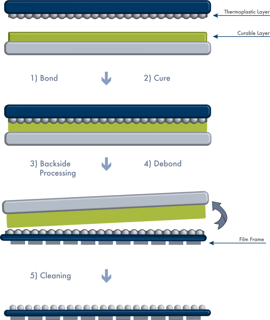
Figure 4. The dual-layer temporary bonding / debonding system by Brewer Science.
Such a dual-layer bonding solution is applicable for high-temperature and high-stress applications, especially those within the semiconductor industry. With innovative materials such as BrewerBOND® T1107 (high-Tg thermoplastic) and BrewerBOND® C1301-50 (curable thermoset), a dual-layer system can exhibit high mechanical and thermal stability (≤ 400 °C), low-temperature bonding (≤ 25 °C), better adhesion at all interfaces, shorter baking time, and higher throughput. Basically, a BrewerBOND® T1100 series material acts as a conformal adhesive coating, while a BrewerBOND® C1300 series material provides the advantages of high-flow, low-pressure, and low-temperature bonding. The table below shows the properties of both materials.
Table 1. The properties and applications of BrewerBOND® T1100 / C1300 series materials.
|
|
BrewerBOND® T1107 material |
BrewerBOND® C1301-50 material |
|
Mechanical Properties |
||
|
2.5 GPa |
3.3 * 10-3 GPa |
|
|
62 MPa |
- |
|
|
Thermal Properties |
||
|
6.3 * 10-5 1/K |
3.9 * 10-4 1/K |
|
|
Glass transition temperature |
328°C |
- 50°C |
|
Maximum service temperature |
465°C |
420°C |
|
Physical Properties |
||
|
Density |
1 g/cm3 |
0.9 g/cm3 |
|
Potential Application areas |
High-temperature adhesives and bonding |
|
Who is Brewer Science?
Brewer Science is a pioneering manufacturing company that develops innovative materials and technologies for industries like semiconductors, electronic packaging, and high-temperature adhesives. Brewer Science was founded in 1981, and since then has enhanced its materials research and technology capabilities into areas of advanced lithography, advanced packaging, and printed electronics. With over a hundred patents and innovative R&D, this global company has also empowered next-generation microdevices and monitoring systems in industrial, environmental, and air applications.
Furthermore, Brewer Science’s dedication to being environmentally friendly and a proponent of sustainability is second to none. It is committed to producing materials with zero defects and zero-waste-to-landfill, earning it the GreenCircle® Zero Waste to Landfill certification for the last five years straight.
Today, Brewer Science has partnered with Matmatch to bring its materials, expertise, and technologies closer to engineers, researchers, and product developers. With selected materials digitised and listed on Matmatch, users can not only view, compare, and examine the material properties but also contact Brewer Science personnel directly with their technical questions and requests.
Visit the Brewer Science supplier profile for more information and get in touch with them directly.

Article by Brewer Science
Brewer Science is a global leader in developing and manufacturing next-generation materials and processes that foster the technology needed for tomorrow. Since 1981, we’ve expanded our technology portfolio within advanced lithography, advanced packaging, and printed electronics to enable cutting-edge microdevices and unique monitoring systems for industrial, environmental, and air applications. Our relationship-focused approach provides outcomes that facilitate and deliver critical information. Our headquarters are in Rolla, Missouri, with customer support throughout the world. We invite you to learn more about Brewer Science at www.brewerscience.com.

Send a question to