Nanofabrication: An Overview
New tools and techniques are in a constant evolutionary path of miniaturisation of electronic components. A few decades ago, component sizes were in the range of tens of micrometers, becoming later in single-digit micrometers, and then in the hundreds of nanometers. Today, the smallest dimensions reached in fabrication vary in the tens of nanometers [1].
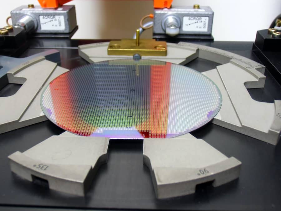
Nanofabrication is the process of producing materials in the nanometer-scale level (i.e. 1 to 100 nm). It is used synonymously with the relatively older term “microfabrication” as the guiding principles have remained the same. Yet, nanofabrication has become the mainstream term due to the newly reached dimensions of the end products. It constitutes one of the most significant advances in modern industry. This technology is focused on producing high-end components, devices, or systems, in large quantity and at potentially low cost [2]. It is mainly used in the microelectronics industry; however, its advantages have also captured the interest of scientists working in the medical, defence, and aerospace industries.
In this article, you will learn about:
- What nanofabrication is
- The different nanofabrication techniques
- The wide-range of nanofabrication applications
What is nanofabrication?
Nanofabrication can be defined as the process of assembling a 1D, 2D, or 3D structure at a scale between 1 and 100 nm in order to utilise unique properties that become evident at these dimensions. As a reference, a nanometer is a unit in the International System that represents 10-9 meter in length.
Nanofabrication, also referred to in the industry as nanomanufacturing, is encompassed by nanotechnology. As its name implies, nanotechnology means “technology at the nanoscale”. It represents the study of chemical, physical, and biological systems at the nanoscale, as well as their integration into nanomaterials or nanostructures.
Nanofabrication techniques
Nanofabrication consists of mainly two major techniques:
Top-down nanofabrication
In this approach, the bulk material or solid is modified or broken into the desired smaller structures using physical (lithographic) tools or chemical processes that deconstruct the material until the final shape and size are achieved [3][4].
Bottom-up nanofabrication
In this approach, materials of atomic or molecular scales are used as building blocks for the formation of nanostructures. This approach is also known as nanomanipulation, describing the process of moving and modifying objects at the atomic/molecular scale [2]. Bottom-up processes are based on thermodynamic and kinetic aspects that define the outcome, as opposed to the deterministic nature of top-down approaches.
The table below presents some examples of nanofabrication techniques [5]. It is important to note that in practice, any nanofabrication technique is not used alone but in a combination with several other processes.
|
Bottom-Up Processes |
Top-Down Processes |
|
Contact Printing |
E-beam, Ion-beam lithography |
|
Template growth |
Scanning probe lithography (SPL) |
|
Spinodal wetting/dewetting |
Optical near field lithography |
|
Laser trapper/tweezer |
Femto-, att-sec laser |
|
Self- and Indirect- assembly |
Material removal process |
|
Electrostatic |
Electro-erosive process |
|
Colloidal aggregation |
Ultrasonic material removal |
Some of the most basic techniques used are briefly described below:
Lithography
Lithography refers to the process where patterns of desired structures are imposed on semiconductor crystals using masks to produce integrated circuits or nanoelectromechanical systems. The new generation of lithography uses x-ray, extreme UV, and charged particles. It also operates in the nanoscale for which it is also known as nanolithography. This process is considered a hybrid between the top-down process of etching and the bottom-up process of nanolayer growth [6].
Etching
Etching refers to the method where the solid surface is modified by dissolving in a liquid or gas (wet etching or electrochemical etching), by applying physical-mechanical methods (dry etching), or a combination of both. In dry etching, the etchant can be either in vapour phase or in plasma phase, resulting in different etching effects [7].
Moreover, etching can be either isotropic (in all directions), anisotropic (unidirectional, following crystal directions), or directional (following the direction of the bombarding etchants).
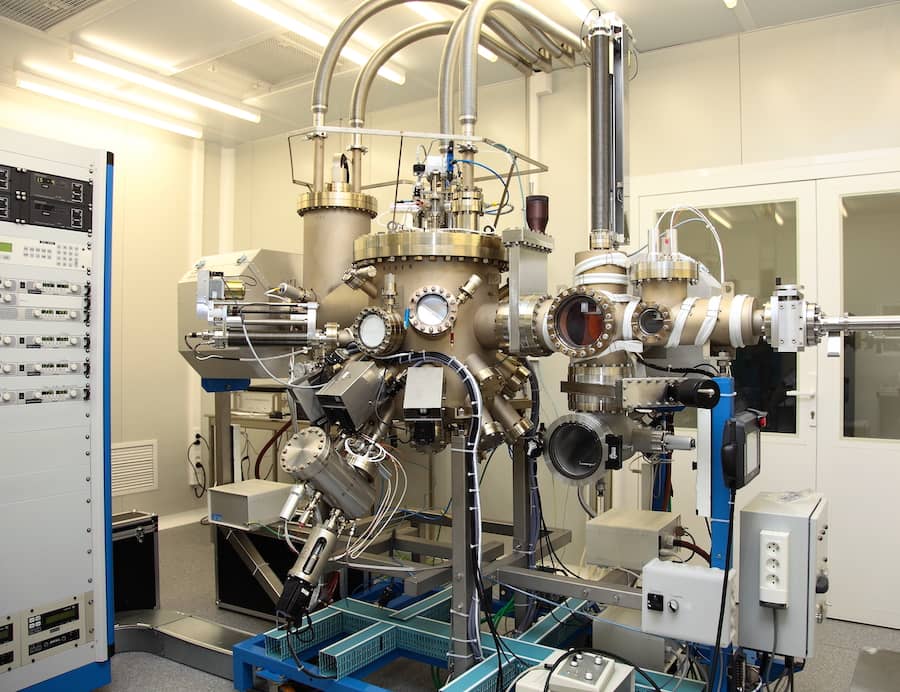
Thin films
Thin films are layers of crystalline structures with nanometer-level thickness. They are fabricated using a variety of deposition coating processes, including chemical vapour deposition (CVD), physical vapour deposition (PVD), atomic layer deposition (ALD), and molecular beam epitaxy (MBE) [8].
Nanofabrication applications
Products created by nanofabrication are in constant development. Industry sectors that are targets for the use of these products include electronics and semiconductors, computing and information technology, communications, defence, automotive, chemical, and medical industries.
Among some of the most common products derived from nanofabrication are [9]:
- Semiconductors
- Nanowires
- Nanostructured particulates
- Nanotubes
- Coatings, paints, and thin films
- Nanoparticles
- Nano/microfluidic systems
- Integrated optics
- Microelectromechanical systems (MEMS)
- Defence, security, and protection gear
- Telecommunications, displays, and optoelectronics products.

Sources
[1] Sarangan, A. (2016), "Nanofabrication", In Fundamentals and Application of Nanophotonics, Woodhead Publishing.
[2] Tseng, A. A. (2008), Nanofabrication: Fundamentals and Applications, World Scientific Publishing Co. Pte. Ltd., Danvers, MA.
[3] Nasrollahzadeh, M., Sajadi, S.M., Sajjadi, M. and Issaabadi, Z. (2019), "An Introduction to Nanotechnology", Interface Science and Technology, Volume 28, pages 1-27, Abstract, [Online].
[4] Yu, H-D., Regulacio, M.D., Ye, M., and Han, M-Y. (2013), "Chemical routes to top-down nanofabrication", Chemical Society Reviews, Issue 14, Abstract [Online].
[5] Biscarini, C., Komanduri, T., Fabio, J., Ranga, C. (2002), NSF-EC Workshop on Nanomanufacturing and Processing, (PDF). National Science Foundation, [Online].
[6] Kumarm D.S., Mahesh, H.M. (2018), Quatum Nanostructures (QDs): An Overview, In: Synthesis of Inorganic Nanomaterials, Woodhead Publishing.
[7] Gatzen, H.H., and Saile V. (2015), Micro and Nanofabrication, Tools and Process, Springer, Germany.
[8] Cui, Z. (2008), Nanofabrication: Principles, Capabilities and Limits, Springer.
[9] Busnaina, A. and Mehta, M. 2006, Introduction to Nanoscale Manufacturing and the State of the Manufacturing Industry in the United States, Nanomanufacturing Handbook.