Modified PEEK for Microsensor Production with LDS Technology
Ensinger
Crystalline silicon wafers have been the materials of choice in the micro-electro-mechanical systems (MEMS) industry for a long time. They have been the cornerstone of many industries that use micro-machines, micro-actuators and sensors, including position sensors, eddy current sensors, and temperature sensors. Despite their widespread use, silicon wafers’ production as a substrate for these micro-devices is still quite complex and time-consuming. Could there be a way to get similar functionality with a much faster and more cost-effective production process using an alternative material?
This question has prompted researchers at the Institute of Micro Production Technology (IMPT) in Hannover, Germany, to find alternative materials that can replace the relatively expensive silicon in the manufacture of these substrates. A new production process has also been developed by LPKF Laser & Electronics AG, which uses laser technology to directly imprint conductive paths on a substrate. The combined result of these two R&D endeavours was a promising modified polyetheretherketone (PEEK) material produced by Ensinger and a simplified production process in laser direct structuring (LDS). Both have exhibited great potential in reducing the cost of production substrates in microsystems technology.
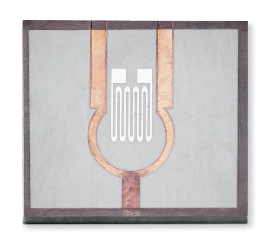
Figure 1. Eddy current sensor. For its manufacture by means of the LDS method, the compound TECACOMP PEEK LDS grey is used. This new product variant from plastics processor Ensinger fulfils particularly high surface requirements (Photo: Ensinger / IMPT).
What is the LDS process?
Conventional silicon wafer production involves an array of complex steps. Instead, this new process that uses injection moulding and LDS can greatly reduce the time and difficulty of manufacture and relax some of the production conditions. For example, LDS does not require a cleanroom environment or the extensive process of photolithography.
The steps of injection moulding and LDS include the following:
Injection moulding
The polymer used for this process is PEEK. It is pre-mixed with mineral fillers or additives that make it laser-activatable, i.e., suitable for LDS at a later stage. The material is moulded to integrate pre-set mechanical designs, which give it structural integrity, and vertical interconnect accesses (VIAs) for electrical connections through adjacent layers of the mould material. Optimal geometrical design ensures that the finished part is reliable and robust. The PEEK material must have excellent injection moulding properties, such as good melt mass flow rate and minimal shrinkage.
Laser direct structuring
Laser direct structuring allows conductive recesses to be directly engraved on the surface of the injection-moulded parts. These conductive outlines are created after the additive-containing polymer substrate is selectively activated/precipitated along a path via a laser beam. Essentially, the conductive pattern is carved directly on the substrate, which now becomes both the component housing and the electronic circuit.
Metallization
In this step, extremely thin layers of conductive metals are successively added along the conductive pattern written by the laser. The readymade pattern provides a rough surface for the metallic material to adhere to. Copper is typically the adopted material here, but other metals, such as gold, nickel, tin, or silver, can be used, as well.
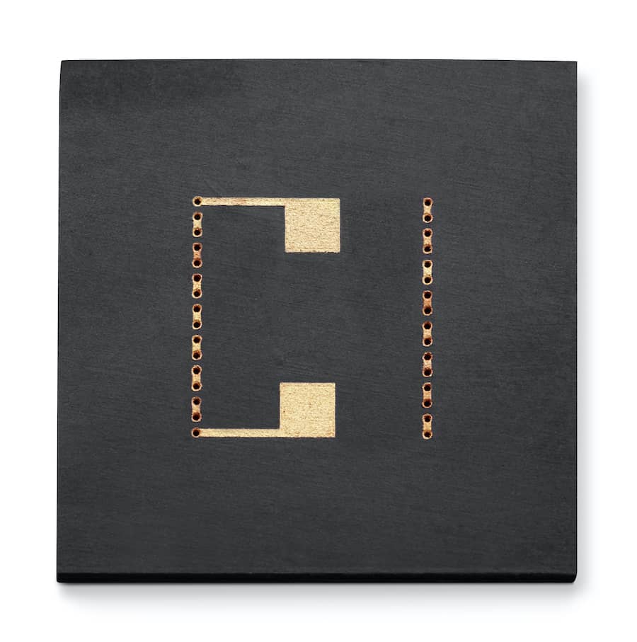
Figure 2. Magnetic field sensor manufactured by means of injection moulding with laser direct structuring (LDS). The substrate used is the high-performance polymer TECACOMP PEEK LDS black 1047045 from Ensinger (Photo: Ensinger / IMPT).
Properties of TECACOMP PEEK for the LDS process
TECACOMP PEEK LDS black 1047045, from Ensinger, has been specially modified for the production process of injection moulding and laser direct structuring for MEMS applications. These production processes, particularly LDS, have very stringent material property requirements, including isotropy and a capacity for metallization.
This is in addition to the similarly strict requirements for materials used in MEMS, in general, such as adequate mechanical and electrical properties, good machinability at a micro level, and resistance to stresses that develop during micro-machining.
TECACOMP PEEK LDS black 1047045 has high-temperature performance (260°C), excellent mechanical strength, good flammability, good weld and adhesive strength, and an exceptionally low coefficient of linear thermal expansion, which is important to ensure the polymer does not disassociate from the metal due to thermal fluctuations. It also displays good chemical resistance to solvents and very low water absorption, an important parameter in wafer production.
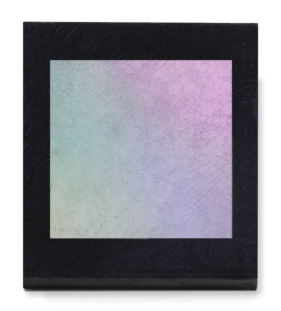
Figure 3. The illustration shows microstructures (Bragg grating) on a sensor. The compound TECACOMP PEEK LDS black 1047045 made by Ensinger is extremely temperature-resistant, has very good weld line strength, good adhesive strength and shows very high chemical resistance to solvents. The material also has a very low coefficient of linear thermal expansion (Photo: Ensinger / IMPT).
The table below shows in more detail the property values of TECACOMP PEEK LDS black 1047045.
Table 1. Material properties of TECACOMP PEEK LDS black 1047045.
|
Property |
Value |
|
Bulk density at 23 °C |
0.9 g/cm³ |
|
Density at 23 °C |
1.67 g/cm³ |
|
Water absorption at 23 °C |
0.10% |
|
10.9 GPa |
|
|
2.50% |
|
|
35 kJ/m² |
|
|
105 MPa |
|
|
Coefficient of thermal expansion at 61.5 °C |
1.8E-5 1/K |
|
Coefficient of thermal expansion at 230 °C |
4.6E-5 1/K |
|
Coefficient of thermal expansion at 280 °C |
6.3E-5 1/K |
|
Coefficient of thermal expansion (transverse) at 61.5 °C |
2.6E-5 1/K |
|
Coefficient of thermal expansion (transverse) at 230 °C |
6.7E-5 1/K |
|
Coefficient of thermal expansion (transverse) at 280 °C |
8.5E-5 1/K |
|
Glass transition temperature |
143 °C |
|
Heat deflection temperature, 1.80 MPa |
218 °C |
|
Max service temperature, long |
260 °C |
|
Max service temperature, short |
300 °C |
|
Melting point |
343 °C |
|
Specific heat capacity at 23 °C |
970 J/(kg·K) |
|
Thermal conductivity, in-plane at 23 °C |
1.7 W/(m·K) |
|
Thermal conductivity, through-plane at 23 °C |
0.5 W/(m·K) |
|
Thermal diffusivity, in-plane at 23 °C |
1 mm²/s |
|
Thermal diffusivity, through-plane at 23 °C |
0.28 mm²/s |
|
Flammability |
UL94 class V0 |
|
Comparative tracking index at 23 °C |
225 V |
|
Dielectric constant, 1KHz at 23 °C |
3.73 [-] |
|
Dielectric strength at 23 °C |
17.5 kV/mm |
|
Loss factor at 23 °C |
6.6E-3 [-] |
|
Surface resistivity at 23 °C |
5.80E+12 Ω/sq |
|
Volume resistivity at 23 °C |
5.80E+12 Ω·cm |
|
Melt mass-flow rate |
77 g/10min |
|
Shrinkage at 23 °C |
0.52% |
|
Shrinkage, transverse at 23 °C |
0.56% |
What makes TECACOMP PEEK LDS black 1047045 really special?
Ensinger has been at the forefront of thermoplastic compounds development for LDS and is currently the only company that produces a PEEK variant that is adapted and certified for the LDS production method by LPKF Laser & Electronics AG. Their compound TECACOMP PEEK LDS black 1047045 was demonstrated by IMPT to perform at 75% efficiency compared to conventional silicon-based sensors in their preliminary tests. It is safe to expect that this can be improved upon with further research.
Furthermore, the cost savings brought about by this material – and LDS – have the potential of reaching 90%, which justifies its use even at a lower efficiency for many applications. This definitely makes PEEK and LDS an option worth exploring.
Visit the Ensinger supplier page for more information on their materials listed on Matmatch and to get in direct contact with them.

Article by Ensinger GmbH
High Performance Plastics: Ensinger Compounds develops and produces high-performance compounds with fillers and additives whose formulations are precisely and individually adjusted in line with the customer’s requirements, making them suitable for a varied range of technical applications.
Our portfolio comprises formulations which are electrically conductive, thermally conductive, abrasion and wear-optimized, detectable and designed to permit laser direct structuring. The structure of the company, the specialization of its employees and its widely diverse machine equipment outfit lends us the flexibility required to offer you optimum service, whether for small quantities or large-scale series production.

Send a question to
Ensinger GmbH
TECACOMP PEEK LDS black 1047045 is an alternative material to silicon in microsensor fabrication. It has shown a performance efficiency of 75% compared to traditional silicon-based microsensors but with a cost-saving potential of 90%.
Applications
Mechanical Systems
Housings
Automotive
General Automotive Parts
Gears
Fluid Systems
Fluid Power Systems
Cylinders
Pumps & Motors
Electronics
Electronic Components
Motors
Energy
Batteries
Battery Anode
Battery Cathode
Heat Recovery
Thermal Management
Heat Sinks
Electrical Engineering
Components For Electrical Equipment
Electric & Electromechanical
Electrical Accessories
Electrical Housing
Power Transmission & Distribution Networks
Other Equipment Related To Power Transmission & Distribution Networks
Sensors
Actuators
Electronic Components Others
Connectors
Industrial Connectors
Printed Circuits
Electronics Assemblies
Telecommunications
Electro Mechanical Components
Optoelectronics
Leds
Transmission
Communications
Telecom Equipment
Mobile Phone
Telecom Accessories
Rf Connectors
Radar
Optics & Imaging
Photography
Camera Parts
Steering Components
Auto Electronics
Combustion Engines
Control Systems
Valve Train
Other Components & Systems Of Internal Combustion Engines
Electric Vehicles
E-Motor
Battery Housing
Wear Parts
Bearings
Plain Bearings
Rolling Bearings
Bearing Cages
Bearings General
Rollers
Seals
Closures
Road Vehicle Systems
Transmissions
Rotary-Reciprocating Mechanisms
Valves
Gate Valves
Pressure Regulators
Hvac
Compressors
Vacuum Technology
Heat Pumps
Body Structure
Bumper
Car Electronics
Braking Systems
Car Interior Components
Aerospace
Bearings For Aerospace
Textile Industry
Textile Machinery
Textile Machinery In General
Semiconducting Materials
Semiconductor Industry